Quick Guide
Workflow
- Design the schematic on the left. Add components from the library and draw wires between pins to define nets.
- Place components on the stripboard on the right. Drag them from the unplaced tray onto the board.
- Resolve conflicts. Place cuts to isolate strips and add wires to connect separated nets.
- Done. When all nets are complete and there are no conflicts, you are ready to solder.
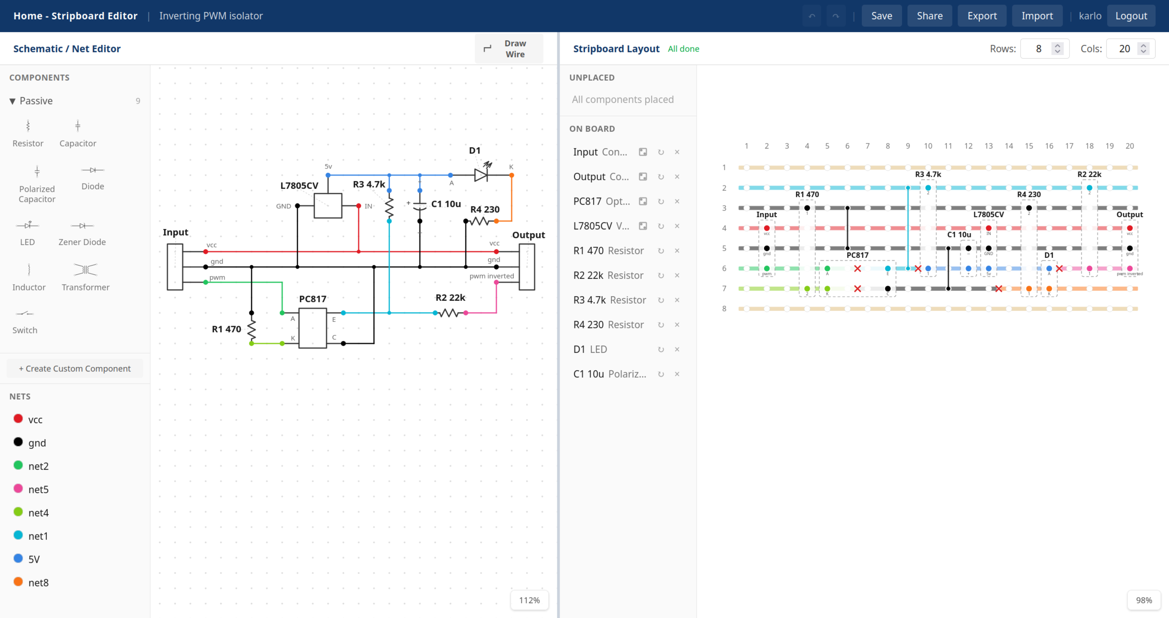
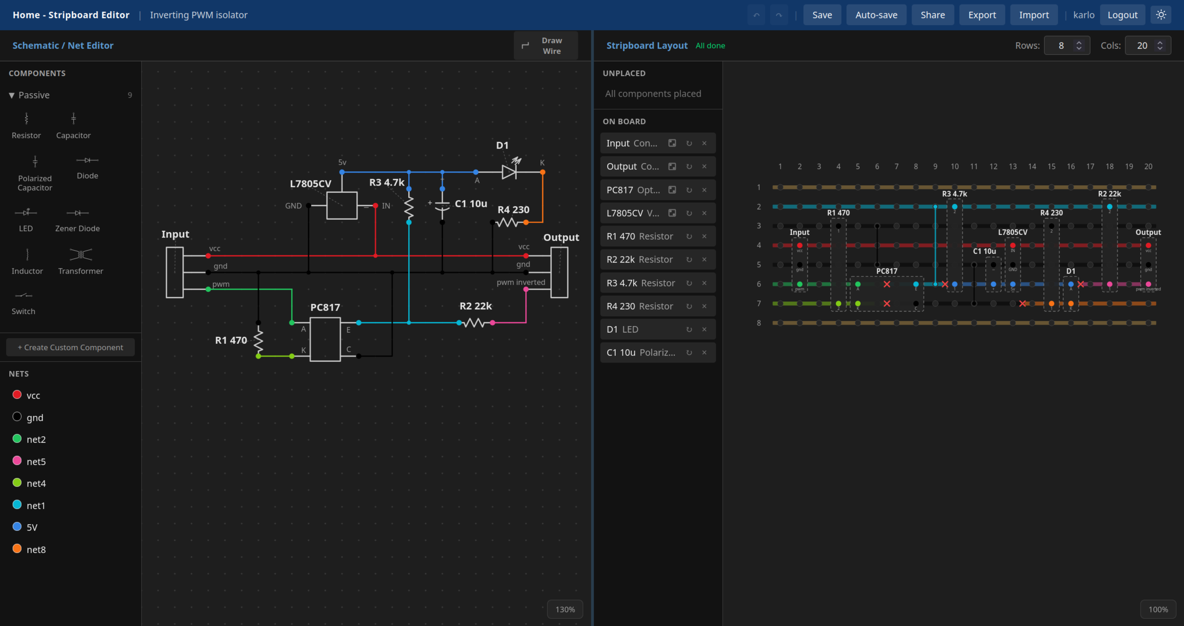
A finished project: schematic on the left, stripboard layout on the right.
Schematic Editor (left)
- Drag components from the library sidebar onto the canvas.
- Click a pin end to start a wire from it, then click pins, wires or grid points to route it. W toggles wire mode, where wires can also start on empty grid. Enter or a double-click finishes a wire, Backspace takes the last segment back.
- Whatever touches is connected: a wire end on another wire, a pin or flag parked on a wire, two pins on the same point. Two wires that merely cross, with neither ending there, stay separate. A dot marks a junction, a small hollow square marks a loose wire end.
- Segments that end up in a straight line with nothing between them are joined into one wire, so editing does not leave a run chopped into pieces. A pin, a flag or a junction always keeps the pieces apart.
- Connected pins automatically form a net. Rename or recolour nets in the sidebar.
- Ground and power flags (G / P, or drag them from the library) and net labels (L) join everything carrying the same name into one net, so GND and VCC need no wires across the sheet. Double-click a flag to rename it.
- Click selects, Ctrl + click toggles, Shift + click adds. A box dragged left to right selects what it encloses, right to left everything it touches. Wires can be selected and moved like parts.
- Click a component label to rename it. Click a pin label to rename the pin.
- Drag labels and pin labels to reposition them if they overlap with wires.
- Select one or more components and press E (or use Exclude in the floating menu) to keep them off the stripboard. Excluded parts stay in the schematic but are ignored by the board and its net checks, so you can draw a full circuit while only building part of it. Press E again to include them back.
- Use the footprint editor (on the stripboard side) to customise a component's physical layout.
Older projects: schematics drawn before touching meant connected follow the rules they were drawn under, where only wire ends connect. Drawings that mean the same thing under both sets of rules were switched over for you. The rest show a Classic wiring link in the schematic header that previews every change the switch would make, down to the individual pins, and applies it. The switch is optional, and undoable.
Stripboard Editor (right)
- Drag components from the Unplaced tray onto the board.
- Placed parts show which way round they sit: a pin-1 notch on ICs, a flat-belly (TO-92 style) outline on 3-legged parts like transistors and voltage regulators, and the USB connector on dev boards such as the ESP32.
- Strips automatically colour to match the net of the pin sitting on them.
- Red highlighted strips indicate a conflict where two different nets share the same strip.
- Place a cut to isolate the strip into sections: click between two holes, or hold Alt and click a hole to cut the strip at the hole itself.
- Click a hole then another hole to place a wire connecting them. Click an existing wire to delete it.
- Wires may run in parallel on the same column or row, as long as they do not share a hole. They shift sideways slightly on screen so each run stays visible. To start a wire on a hole that sits under an existing wire, hold Shift while clicking: clicks then pass through wires straight to the holes underneath.
- Right-click a row or column number to insert a blank row or column, or to delete one. Inserting shifts everything past the line and stretches parts and wires spanning it. Deleting removes the wires and cuts on that line and unplaces any component with a pin or body on it; parts and wires merely spanning the line shrink to close the gap.
- A hole holds either a cut or a wire, never both. Click a hole cut to remove it (no Alt needed).
- 2-pin passive components (resistors, LEDs, etc.) have flexible leads. Drag individual pins to reshape them.
- Non-flexible components (ICs, connectors, etc.) can have their footprint edited. Select a placed component, then click Edit Footprint in the floating menu above it. You can resize the grid and move pins around to match your physical component.
- Hover over an incomplete net in the sidebar to highlight the relevant strips.
Auto-layout
Click Auto-layout in the stripboard toolbar. The layouter places every part, picks the board size, and adds the cuts and link wires. If anything cannot be completed, a pop-up tells you what and why.
- Lock the board size. Click the padlock next to Rows or Cols to keep exactly that many. A locked board cannot grow, so a few slanted or crossing wires may remain.
- Lock parts. Select placed parts and press L to keep them where they are. Locked layouts come out a little larger.
- Settings (gear beside the button): pin spacing and clearance per flexible part type, drilled cuts only, no stacked wires, how many layouts to solve, and the anneal effort per layout. Each option explains itself in the panel.
Curious how it decides all this? How auto-layout works →
Printing & Assembly
- Click Print in the project toolbar to open the print / PDF dialog and generate an assembly guide.
- The component sheet shows the board from the component side. Lay it on top and push leads through the marked holes.
- The cut sheet is mirrored for the copper side and marks every track cut with an .
- The BOM (bill of materials) lists quantities, values, and reference labels for sourcing parts.
- Toggle reference labels, wires, cuts, and pin labels to tailor each sheet to your build.
- Optionally add a view or edit QR code that links back to the online project.
- Print at 100% / actual size and verify the calibration ruler so hole spacing matches real stripboard.
Exporting
- Open Export in the project toolbar and pick Raw project to download the whole project as a JSON file. Bring it back any time from the Import menu.
- Pick Netlist to export a KiCad-compatible netlist. It carries your components, their reference labels and values, the pin numbers, and every net, so a circuit you prototyped here can go into an EDA tool and become a PCB.
- Most built-in parts map to real KiCad symbols and through-hole footprints, so the netlist imports straight into the PCB editor without hunting for footprints.
- Parts with no standard KiCad footprint (custom components, the dev boards, and a few generic parts) are covered by a small footprint library that downloads alongside the netlist as a zip. Unzip it and add the folder once under Preferences → Manage Footprint Libraries, using the nickname shown in the pop-up.
- A netlist describes connections rather than drawings, so your schematic layout and stripboard placement are not part of it.
- Importing a netlist is not supported yet. For now the editor reads its own project files only.
Keyboard Shortcuts
Custom Components
Click + Create Custom Component at the bottom of the library. Define the grid size, place pins, and assign names. Your custom components are saved with the project and appear in a dedicated Custom section.
Saving & Sharing
- No account is required. When you save a project for the first time, a unique link is generated. Bookmark or save this link to return to your project later.
- You can also export your project as a JSON file from the Export menu and re-import it at any time.
- Creating an account lets you access all your projects from a central dashboard without needing to save individual links.
- Logged-in users can share projects. Each project has an edit link for full access and a separate view-only link for sharing with others.
- Anyone viewing a shared project can fork it to create their own editable copy.